2023 S2 Engineering Capstone Project
Simplified Silicon Foundry at The University of Melbourne
Project Gallery
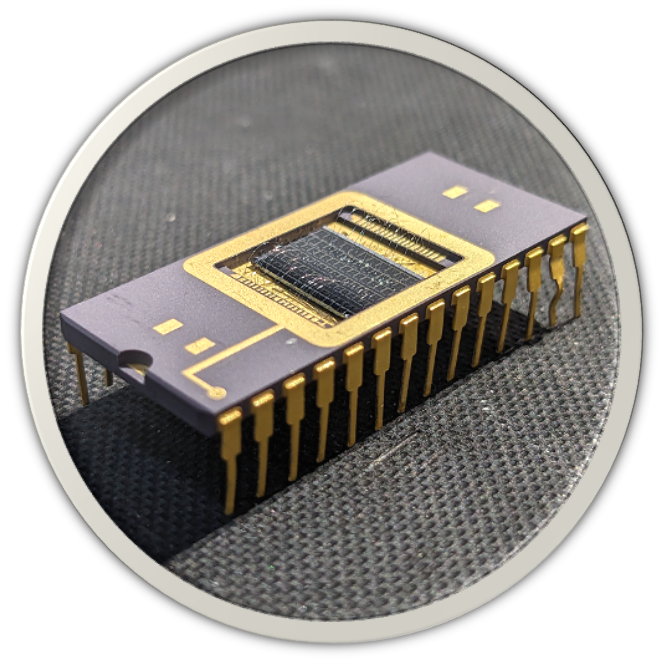
Finished Product
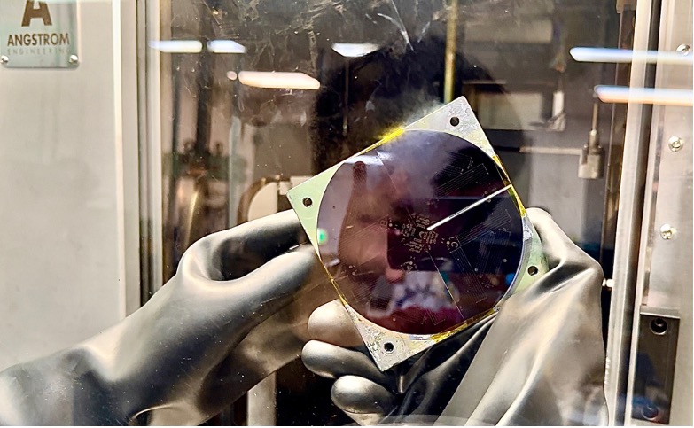
Silicon Wafer with Design
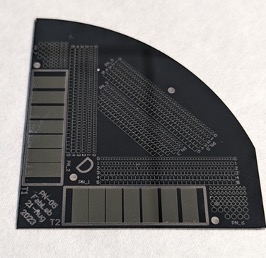
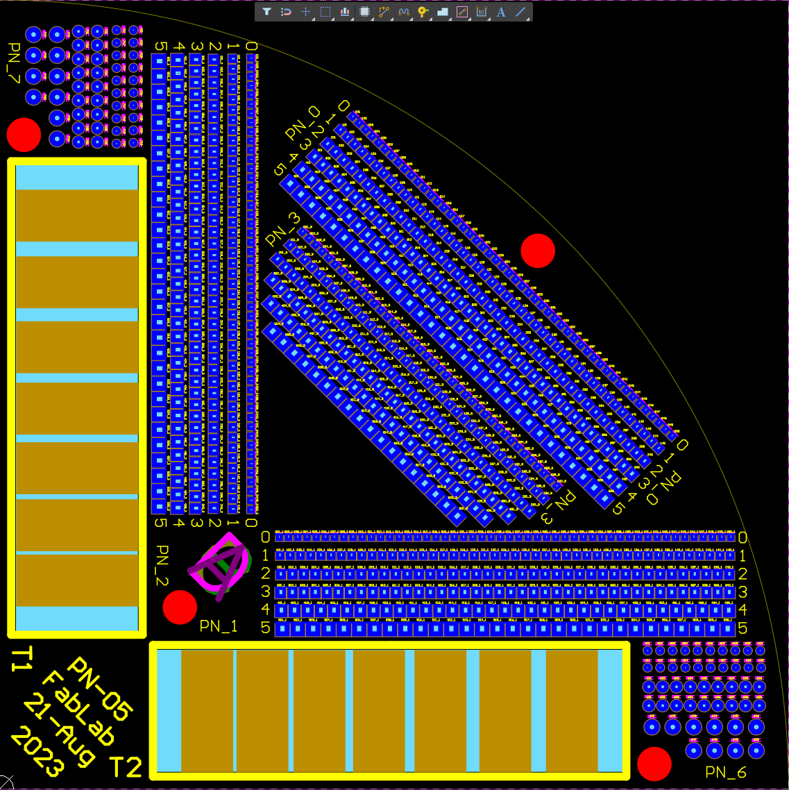
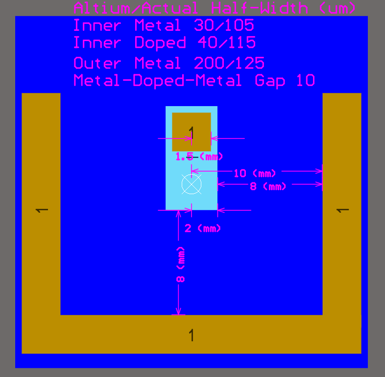
Wafer Design
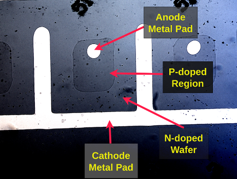
PN Junction
PVD (Physical Vapour Deposition)
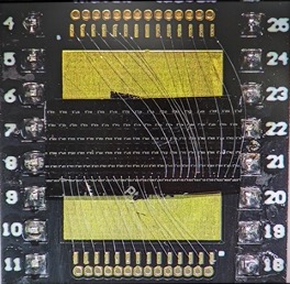
Device with Wire Bonding
Wire Bonding

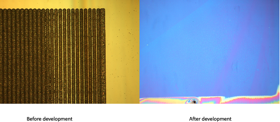
Photoresist

Photoresist before/after Development
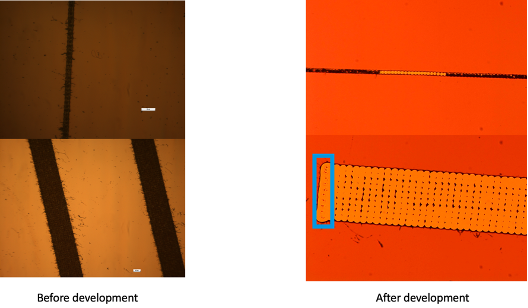
Photoresist before/after Development
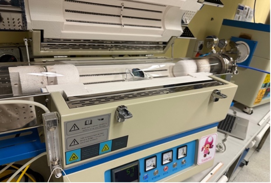
1000ºC Furnace
PN Junction Design
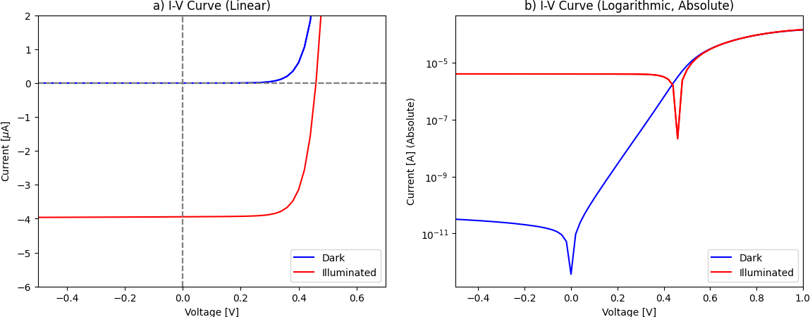
IV Curves
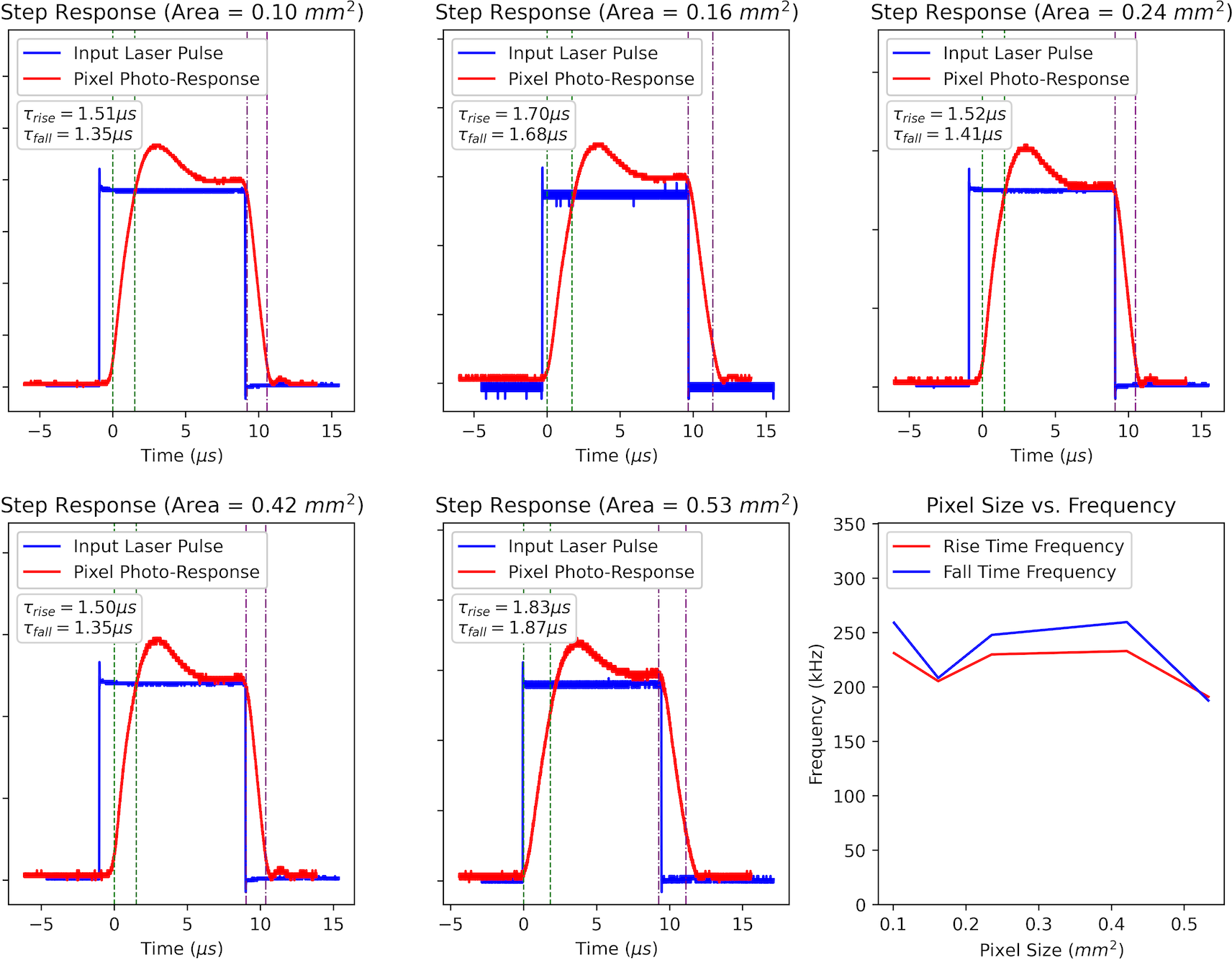
Step Response
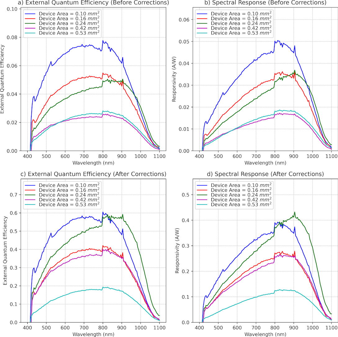
EQE
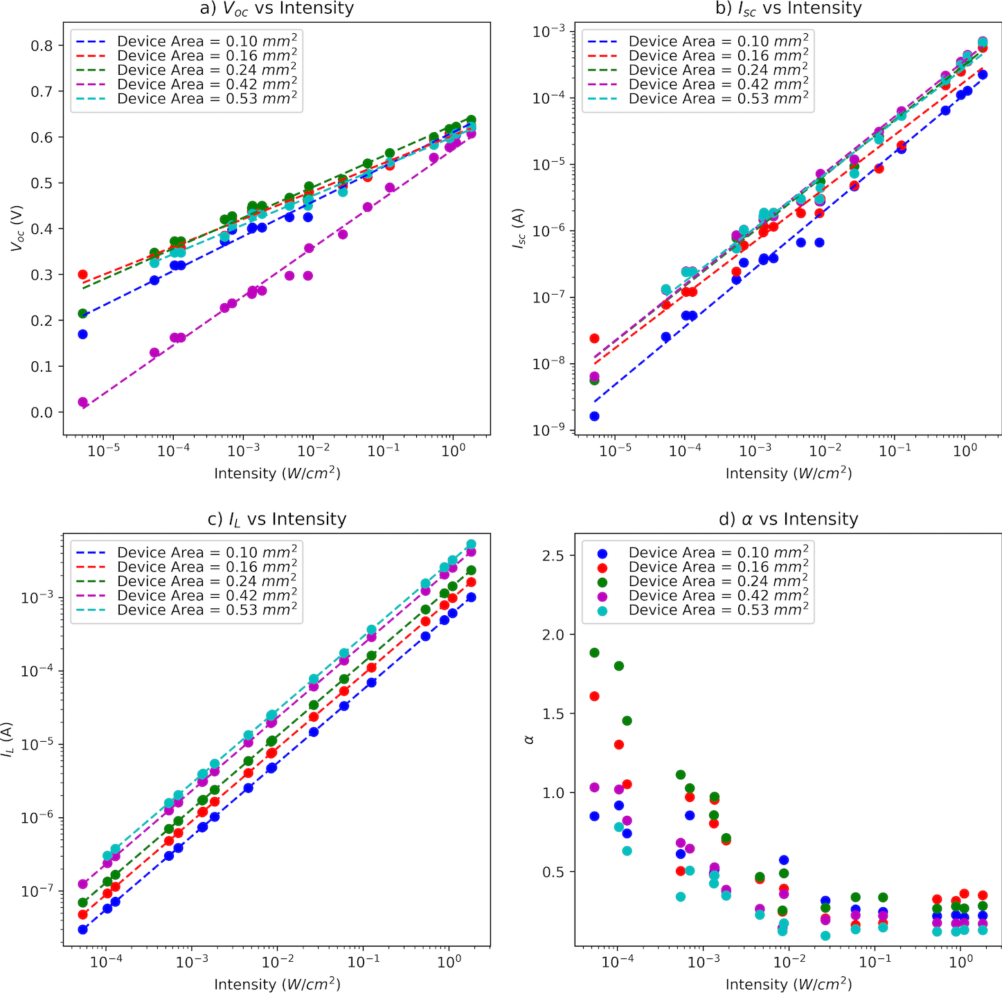
VOC ISC vs Intensity